General Information
The Laboratory of Hybrid Nanophotonics and Optoelectronics is established under open “Megagrant” competition of the Russian Federation
More news on our Twitter
Research areas
1. Development of methods for creating silicon, dielectric and hybrid nanostructures
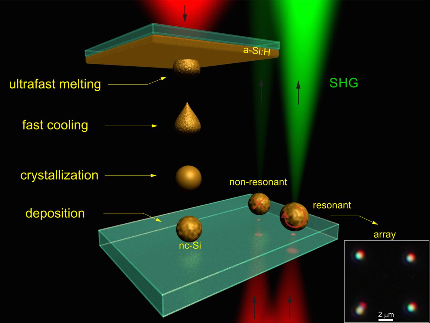
- Formation of silicon nanostructures: It is found that the use of laser pulses allows the creation of a variety of silicon nanostructures.
- Precision laser tuning of nanoantennas: Experimentally and theoretically demonstrated the possibility of precision laser tuning of a hybrid nanoantenna (metal-dielectric), which opens new perspectives for optical recording of colour information.
- Methods of creation of dielectric and hybrid nanostructures: Methods of high-performance creation of dielectric and hybrid nanostructures for nanophotonics have been developed.
- Optimisation of the method of laser printing of nanoparticles: The method of laser printing of nanoparticles for obtaining crystalline silicon nanoparticles from amorphous films was applied and optimised.
- Creation of subwavelength white light sources: Laser printing of gold-silicon nanoparticles enables the creation of subwavelength white light sources.
- Development of a near-field microscope: A white-light near-field microscope has been developed that outperforms commercially available microscopes in scanning speed.
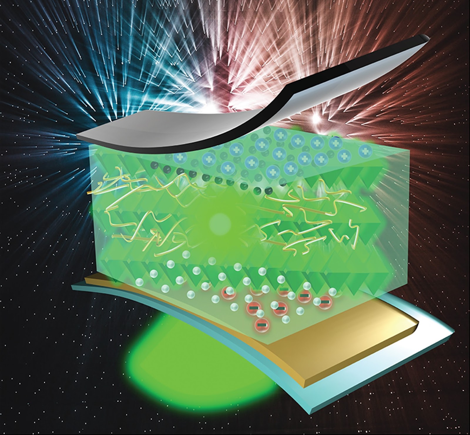
- Perovskite nanophotonics: A new research area, perovskite nanophotonics, was initiated, where halide perovskites are used to develop a platform for optical signal generation, transmission and modulation.
- Understanding nonlinear interactions: The results of the study expand the knowledge of nonlinear interactions of high-power laser pulses with materials, which has applications in the fields of photonics and optics.
- New methods for creating nanostructures: The developed methods for creating dielectric and hybrid nanostructures provide new tools for nanophotonics and advanced laser technologies.
- Technological innovations: The optimised method for laser printing of nanoparticles, the development of sub-wavelength light sources as well as the white-light near-field microscope represent technological innovations with potential in various fields of science and industry.
- New perspectives in optical recording: The possibility of precision laser tunability of nanoantennas opens up new perspectives in optical recording of colour information.
- Perovskite nanophotonics: Initiating the field of perovskite nanophotonics can lead to the development of new materials and devices with high efficiency in the generation and modulation of optical signals.
2. Synthesis of filamentous nanocrystals and study of their properties
Research Objective:
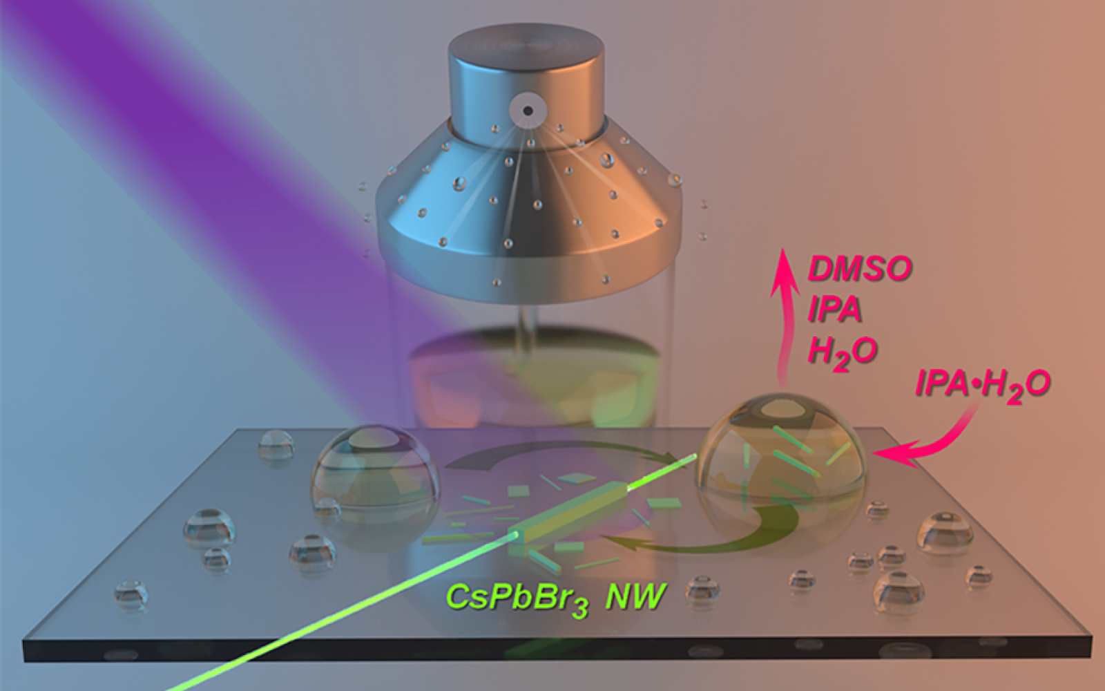
- Method for synthesis of filamentous nanocrystals: A simple method for synthesising high-quality filamentous nanocrystals on nanostructured substrates has been developed.
- Laser oscillators: The obtained nanostructures were found to be suitable for the construction of laser oscillators, which opens prospects for the realisation of laser generation using electric pumping.
- Chemical vapour-anion exchange procedure: Studies on the application of chemical vapour-anion exchange procedure to thin films and filamentary perovskite nanocrystals have been carried out.
- Creation of CsPbBr1.5I1.5 nanostructures: It was determined that the exchange procedure leads to the creation of CsPbBr1.5I1.5 nanostructures based on a mixture of perovskite halides.
- Photoluminescent properties: The photoluminescent properties of the obtained structures have been studied to determine their potential for use in perovskite photonic structures and devices.
- A new method for synthesising nanocrystals: The developed method for synthesising high-quality filamentous nanocrystals represents a new approach to obtain structures with potential for use in laser generators.
- Prospects of laser generation with electric pumping: It is found that the nanostructures obtained from the study can be used to create laser generators using electric pumping, which opens up prospects in the field of optoelectronics.
- Development of perovskite photonic structures: Studies on the creation of CsPbBr1.5I1.5 nanostructures and the study of their photoluminescent properties contribute to the development of perovskite photonic structures with potential in solar cells, light-emitting diodes and other devices.
Research Objective:
Research Results:
- Optical pump lasering: Using chemical synthesis and laser ablation techniques, optical pump lasering with high gain was achieved.
- Terahertz radiation generation: Nanostructured films made of organic-inorganic materials allowed for the first time to achieve enhanced terahertz radiation generation.
- Ultrafast modulation of the optical signal: Ultrafast modulation of the optical signal in resonant nanoparticles of organic-inorganic materials with pronounced exciton states at room temperature was achieved.
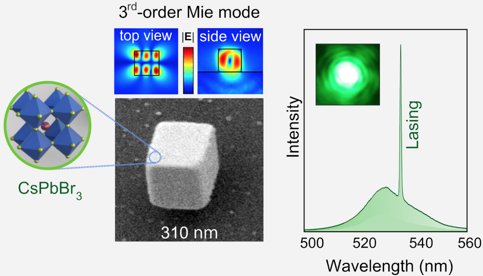
- Nanolasers based on resonant Mie modes: The direction of using low-order resonant Mie modes to create compact nanolasers capable of operating at room temperatures is developing.
- The world's most compact semiconductor laser: The world's most compact optically pumped semiconductor laser (310 nm cuboid) operating at room temperature in the visible range (emission wavelength around 530 nm) was demonstrated.
Scientific value of the results:
- Technological methods: The developed methods of chemical synthesis and laser ablation present new technological approaches to create optically resonant structures with high gain.
- New possibilities for laser generation: The results of the study open new perspectives for laser generation using electric pumping and terahertz radiation generation.
- Exciton states at room temperature: Achieving pronounced exciton states at room temperature in resonant nanoparticles of organo-inorganic materials provides new opportunities for optical devices and applications.
- Compact nanolasers: The development of the use of Mie resonance modes to create compact nanolasers at room temperature opens up new possibilities for the integration of laser devices into micro- and nanosystems.
4. Integration of perovskite microcrystals with gallium phosphide nanofibres
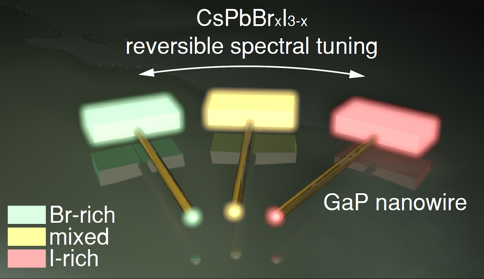
- Platform for visible light: A platform combining a perovskite light source with optical nanowaveguides made of III-V semiconductors has been developed, operating in the visible range.
- Hybrid structure: A hybrid structure based on high-quality filamentary gallium phosphide (GaP) nanocrystals embedded in CsPbBr3 microplates was developed.
- Efficient integrated circuit for visible light: A highly versatile and efficient integrated circuit for visible light is developed, providing tunable integrated light sources.
Value of the results for science:
- Integrated Photonics Platform: The developed platform represents an important step in the field of integrated photonics, enabling the combination of various light sources with optical nanowaveguides.
- Low-loss hybrid structure: The developed hybrid structure combines high-quality filamentous nanocrystals with an indirect-gap semiconductor and perovskite microplates to provide coupling efficiency and low waveguide losses.
- Broadband wavelength tuning: The ability to broadband tune the emission wavelength in the integrated circuit provides flexibility for a variety of optics and lighting applications.
- Versatile integrated circuit for visible light: The developed integrated circuit with tunable light sources provides a versatile solution for building sophisticated optical devices in the visible range.
5. Methods of depositing composite layers on various substrates
- Methods for integration of halide perovskites: Methods for integration of halide perovskites with metal-organic frameworks, hyperbolic metamaterials and flexible substrates have been developed.
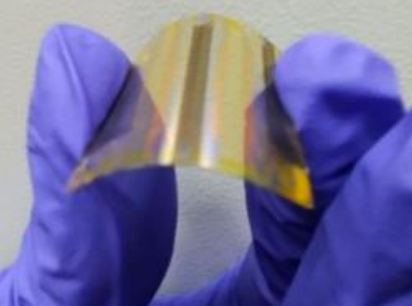
- Optoelectronic devices on flexible substrates: Various optoelectronic devices, such as electrochemical cells and photodetectors, on flexible PET polymer substrates using stable carbon electrodes (carbon nanotubes) have been created.
- Semitransparent carbon devices: The use of flexible substrates together with translucent carbon nanotube electrodes allows the creation of translucent carbon devices that function effectively on bendable or transparent surfaces.
Scientific value of the results:
- Development of composite layer deposition methods: The developed composite layer deposition methods represent a significant contribution to the field of nanotechnology and the development of functional materials for optoelectronic devices.
- Integration of perovskites with various materials: Integration of halide perovskites with organometallic frameworks, hyperbolic metamaterials and flexible bases opens new perspectives for creation of advanced and multifunctional materials.
- Development of optoelectronic devices on flexible substrates: The developed optoelectronic devices on flexible substrates have potential for a variety of applications, including electrochemical cells and photodetectors on flexible surfaces.
- Semitransparent carbon devices: The development of semitransparent carbon devices opens up new possibilities for efficient devices that can be used on surfaces with different optical characteristics.
6. Light-emitting optoelectronic devices with electrochemical cells
- Pin-structure within the active layer: A device design with pin-structure inside the active layer of CsPbBr3:PEO:LiPF6 has been developed, without the need for transport layers.
- Mechanism of operation under electric bias: Under an applied electric field, the drift of anions (Br- and PF6-) and cations (Li+ and Cs+) leads to the formation of p- and n-type doping and the formation of a p-i-n junction. This provides improved charge transfer and efficient device performance.
- Light-emitting perovskite cells: Efficient light-emitting perovskite cells have been assembled using the described mechanism of operation under electric bias.
- Innovative device design: The developed pin structure within the active layer is an innovative approach that eliminates the need for transport layers and improves device performance.
- Understanding the mechanism of operation: The detailed description of the mechanism of operation of light-emitting perovskite cells under electrical bias makes an important contribution to the understanding of the physical processes in these devices.
- Efficient light-emitting cells: The results obtained on efficient light-emitting perovskite cells provide a practical contribution to the development of light-emitting perovskite devices and their applications in optics.
7. Multifunctional devices based on halide perovskites
Research Objective:
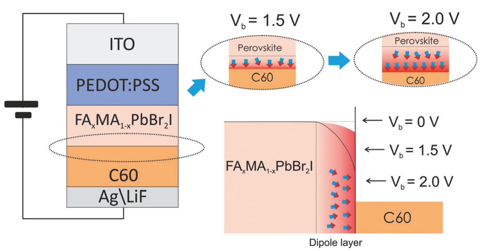
- Light-emitting perovskite halide-based solar cell: A light-emitting solar cell has been developed that can switch between modes thanks to controlled ion migration within the active layer.
- Mixed anion: The presence of organic MA+ or FA+ cations with non-zero dipole moment in the perovskite composition allows the formation of a dipole layer at the perovskite interface and an electron transport layer.
- Mode switching: The mechanism of controlled ion migration and dipole layer formation allows the device to switch from solar cell operation to LED mode and back.
Value of the results for science:
- Multifunctional devices: The developed light-emitting solar cell is an example of a multifunctional device capable of performing various functions such as power generation, photodetection and LED lighting.
- Controlled ion migration: The mechanism of controlled ion migration within the active layer represents a new way to control the functionality of perovskite devices, opening up prospects for more efficient and flexible devices.
- Mode switching: The ability to switch the device between solar cell and LED modes of operation depending on conditions provides new opportunities to optimise the energy efficiency and functionality of perovskite-based devices.
8. Optimisation of solar cells based on halide perovskites
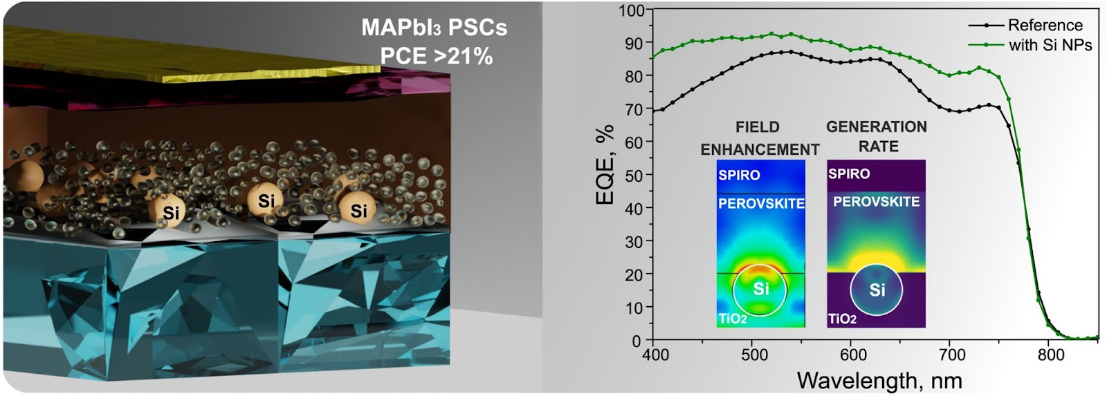
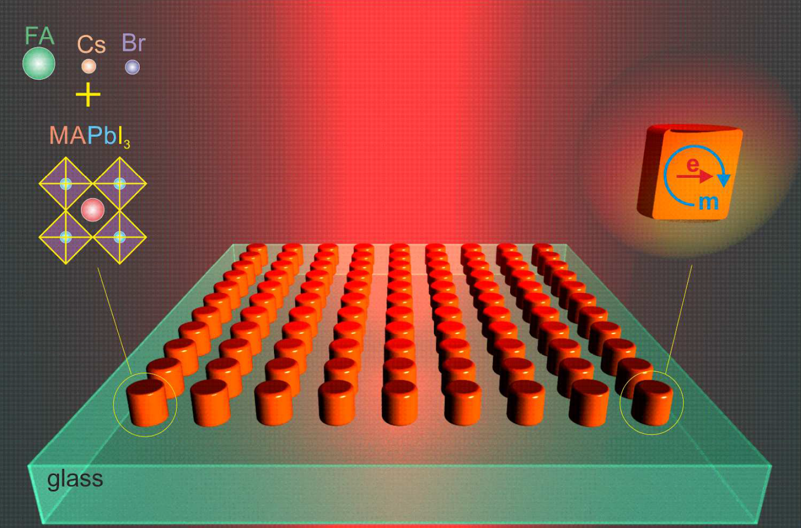
- Nanostructuring of halide perovskite layer: Studies have shown that nanostructuring of halide perovskite layer using introduction of nanoparticles such as silicon nanoparticles results in imparting metasurface and metamaterial properties, which helps in improving the efficiency of solar cells.
- Integration of silicon nanoantennas into perovskite devices: The concept of integrating silicon nanoantennas into perovskite optoelectronic devices was developed, which improved the solar cell efficiency up to 21%.
- Synthesis of high efficiency perovskite solar cells: High efficiency perovskite solar cells with efficiencies up to 19.4% were synthesised using optimised halide perovskite MAPbI3 and an optimised device architecture with PTAA and PCBM transport layers.
- Optimisation of architecture using anti-reflective coatings: Optimisation of solar cell architecture using anti-reflective coatings was carried out, resulting in achieving a photovoltaic conversion efficiency of 29.6%.
- Application of carbon nanomaterials: The application of carbon nanomaterials such as fullerenes and carbon nanotubes as an alternative to metal electrode has been investigated. It has been shown that the combined use of carbon nanomaterials with ionic liquid can compensate the high resistance and use them as electrodes.
- Improvement of solar cell efficiency: The results of the study lead to improved solar cell efficiency, which is important for the development of renewable energy.
- New integration concepts: Silicon nanoantenna integration concepts and the use of carbon nanomaterials present new approaches to develop multifunctional and efficient perovskite devices.
- Optimisation of architecture with anti-reflection coatings: Optimisation of architecture with anti-reflection coatings contributes to the development of more efficient solar cells with high photovoltaic conversion efficiency.
- Application of carbon nanomaterials in electrodes: Exploring the application of carbon nanomaterials in electrodes expands the possibilities of using these materials in solar cells and other optoelectronic devices.
9. Optimisation of tandem devices based on halide perovskites
Research Objective:
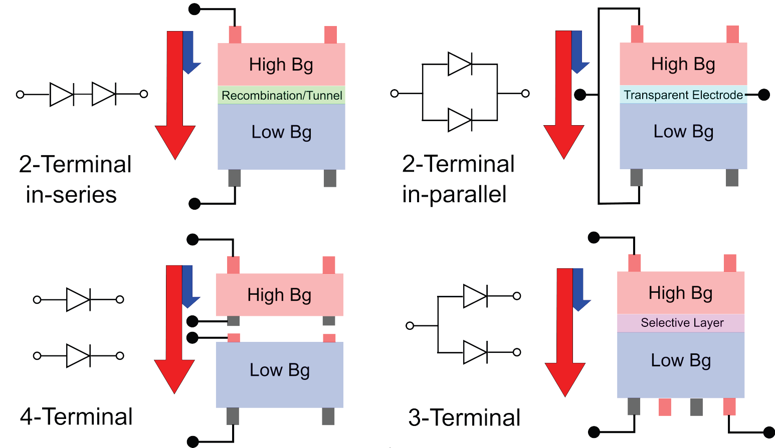
- Tandem solar cells: Using a top cell made of MAPbI3 perovskite and a bottom cell made of silicon heterostructured solar cell, a photovoltaic conversion efficiency of 24.62% was demonstrated. A four-terminal switching scheme was preferred for the parallel connection of the solar cells.
- Light-emitting devices: Light-emitting devices based on electrochemical cells with ITO/CsPbBr3:PEO:LiTFSi/MWCNT architecture were developed. The devices exhibited 50% translucency and luminance of more than 1600 cd/m2. The emissive layer had a transparency of 80%, which contributed to the effective shading of the silicon heterostructured solar cell.
- Flexible LED tandem: Using organic compounds based on platinum complexes, a prototype flexible LED tandem with excimer-like emission was developed. This emission could change colour from red-pink to white depending on the applied electrical voltage.
- Synthesis of carbon nanodots: A method of synthesis of carbon nanodots was developed, providing white photoluminescence with a continuous spectrum from 450 to 1600 nm.
- LED/PV sensor: Organic light-emitting diodes and photodiodes were fabricated to create LED/PV sensor. The proposed sensor allows monitoring of vital human parameters, such as blood saturation, using a single wavelength LED and a photodetector.
- Tandem solar cells: The presented results contribute to the development of tandem solar cells with high photovoltaic conversion efficiency.
- Light-emitting devices: The light-emitting devices developed provide new opportunities in the field of electrochemical cells and can be used in heart rate monitors and other devices.
- Flexible LED tandem: The developed flexible LED tandem with excimer-like emission is of interest for various applications requiring colour change of light.
- Synthesis of carbon nanodots: The method of synthesising carbon nanodots can be an important contribution to the field of creating materials with tailored photovoltaic properties.
- LED/PV sensor: The developed LED/PV sensor may have promising applications in medical devices for monitoring human health.
- 17.12.2020, Candidate of Physical and Mathematical Sciences Zograf Georgiy Petrovich ‘Spectroscopy of enhanced and temperature-sensitive Raman scattering of optically resonant semiconductor nanoparticles’.
- 21.12.2020, Candidate of Technical Sciences Tatyana Gennadyevna Lyashenko ‘Suppression of photo- and electro-induced phase instability in lead-halide perovskites for development of light-emitting devices’.
- 30.06.2021, Candidate of Physical and Mathematical Sciences Al-Naima Hadi Karim Shamkhi ‘Configuration of scattering indicatrix of nanostructures supporting excitation of high order multipole moments’.
- 20.12.2021, Candidate of Physical and Mathematical Sciences Alexander Berestennikov ‘Optical resonances in nanostructures for modification of radiation recombination in halide perovskites’.
- 15.12.2021, Candidate of Physical and Mathematical Sciences Furasova Alexandra Dmitrievna ‘Resonant semiconductor nanostructures for increasing the efficiency of perovskite solar cells’.
- 09.12.2022, Candidate of Physical and Mathematical Sciences Markina Daria Igorevna ‘Spectrally tunable laser generation in lead-halide perovskite filamentary micro- and nanocrystals’.
- 30.08.2023, Candidate of Physical and Mathematical Sciences Masharin Mikhail Alekseevich ‘Stabilisation of p-i-n structure in solar cells based on mixed halide perovskites’.
- 27.11.2023, Candidate of Physical and Mathematical Sciences Pavel Andreevich Tonkaev ‘Control of speed and intensity of radiative recombination in structures based on halide perovskites’.
- 23.11.2023, Candidate of Technical Sciences Grigory Andreevich Verkhoglyadov ‘Investigation of ion migration in organic-inorganic perovskites for realisation of solar cells and LEDs’.
- Vyacheslav Korolev ‘Enhancement of THz emission of MAPbI3 thin films by nanoimprint lithography’
- Artem Polushkin ‘Direct laser writing for creation of perovskite microdisk lasers’
- Evgenia Vadimovna Grechaninova ‘Enhancement of superfluorescence in Mi-resonant superlattices based on CsPbBr3 nanocrystals’
- Bodjago Elena Vasilievna ‘Research and development of semitransparent light-emitting electrochemical cells with multi-walled carbon nanotubes as an electrode’.
- Ralina Rifkatovna Salikhova ‘Investigation of photoluminescence efficiency of perovskite-polymer materials’.
- Anna Aleksandrovna Obraztsova ‘Light trapping in perovskite solar cells due to nanostructuring’.
- Nikita Vyacheslavovich Glebov ‘Control of exciton-polariton dispersion in photonic crystal waveguides fabricated by atomic force lithography of quasi-dimensional perovskite (PEA)2PbI4’.
- Ryabov Daniil Romanovich ‘Nonlinear Optical Heating of All-Dielectric SuperCavity: Efficient Light-to-Heat Conversion through Giant Thermorefractive Bistability’.
Annual PeroFest
PeroLab team and participants of Summer Workshop (2017)
Lab members with lead scientist Anvar Zakhidov at the MOST conference (2024)